 Organization
 |
|
|
|
|
| Activities |
|
|
|
|
|
|
|
|
|
|
| Contact |
|
|
|
|
|
|
| Offers for students |
|
|
|
|
| Departments |
|
|
|
|
|
|
|
|
|
|
|
|
Martin-Luther-University
Interdisziplinäres Zentrum für Materialwissenschaften
Nanotechnikum Weinberg
Heinrich-Damerow-Str. 4,
D-06120 Halle, Germany
|
|
High-resolution electron-microscopic analytics on thin layer materials based on silicon (BMBF-project 03SF0352F - SINOVA)
Project overview SINOVA
Having a market volume of nearly 90 %, solar cells made of crystalline silicon depict the technological basis for the currently rapidly growing photovoltaic industry. The new thin layer technologies made of amorphous and microcrystalline silicon will take over an increasing fraction of the maket volume because of their price advantage. Hence the element silicon and the materials combinable with it provide the dominating material basis of the photovoltaic industry, today as well as in the future. The laboratory record (efficiency) for amorphous or microcrystalline silicon thin layer solar cells, respectively, currently amounts to around 14%, whereby already tandem and triple concepts were applied. Thus, the task of the research community is to procure short- and medium-term possibilities in order to increase the efficiency and to fabricate thin layer solar cells cheaper. But in the long term, physical and technological possibilities allowing efficiencies above the Shockley-Queisser limit have to be developped also for commercial products.
An approach to achieve this purpose is provided by the modification of the silicon material properties through implementation of adequate nano-structures which are smaller than the wavelength of the electron wave function. In this case, quantum confinement effects occur which change the electronic and optic properties of the silicon material dramatically: the electronic density of states is changed, the band-gap energy increases which influences the character of the optic absorption positively. Theoretic estimations exhibit the enormous potential of integrated silicon quantum structures.
Further incipient technology approaches contain the the application of self-organising silicon nano-wire arrays which either may act as absorbers in novel solar concepts or also may be used directly as solar cells for certain niche applications in sensor technology or mobile electronics.
Besides the monocrystalline silicon, its natural oxide, the amorphous SiO2, ranks among the best known silicon compounds. In addition the amorphous silicon, especially the n- and p-dopable a-Si:H with variable hydrogen concentration, plays an important role as amorphous solid and also in thin layer applications. Furthermore, the SiOx(:H) with 0 < x ≤ 2 possesses a potential so far not exhaustet as passivation layer, as possible thin layer emitter or as pre-stage of silicon nano dot absobers.
SINOVA shall investigate different possibilities of nano-structured materials on the basis of silicon and its compatible compounds (SiOx, SiNx, SiC, SiGe) in order to use them as functional elements in high efficient solar cells. The aim of SINOVA is the fabrication of all of these functional elements basing on nanostructured silicon compounds. The central technologic work packages are in this connection (i) the fabrication of a photovoltaic absorber material out of silicon nano structures embedded in a SiO2 matrix and (ii) the fabrication of selective p-type and n-type contact materials consisting of a mixture of silicon nanocrystalls and a SiO2 matrix. These contact materials shall be applied to crystalline wafer solar cells as well as to thin layer solar cells consiting of amorphous and/or microcrystalline silicon.
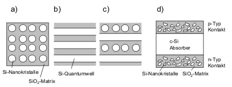 |
| (a)-(c) Different options for the fabrication of Si/SiO2-metamaterials as photovoltaic absorber. (d) Solar cell with selective contacts made of nanocrystalline silicon embedded in a SiO2-matrix. |
Contributions of IZM to SINOVA
- EELS-characterisation of SiOx as substoichiometric barrier material
- Analytical elektron microscopy at Si-nanostructure-absorbers
- EELS at amorphous Si-quantum structures
- EELS-characterisation of the barrier materials Si3N4, ONO (oxide - nitride - oxide) and SiC
- Analytics on OES (oxide embedded silicon)
- Diagnostics on doped nanodot layers
- EELS-investigations towards LIC (light induced crystallisation)
- EELS-investigations on Si-polymorphs (metastable high pressure phases)
Methods
Examples
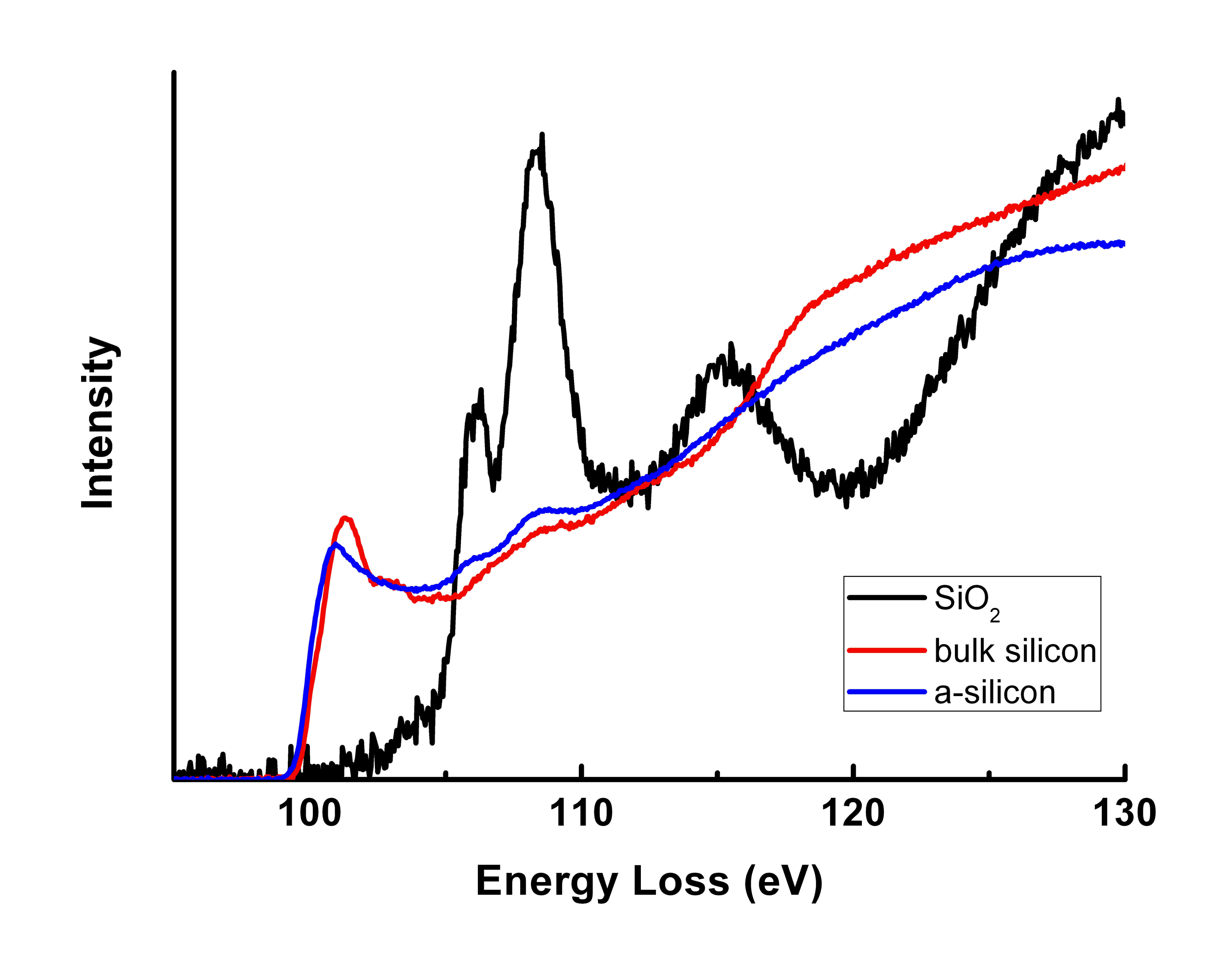
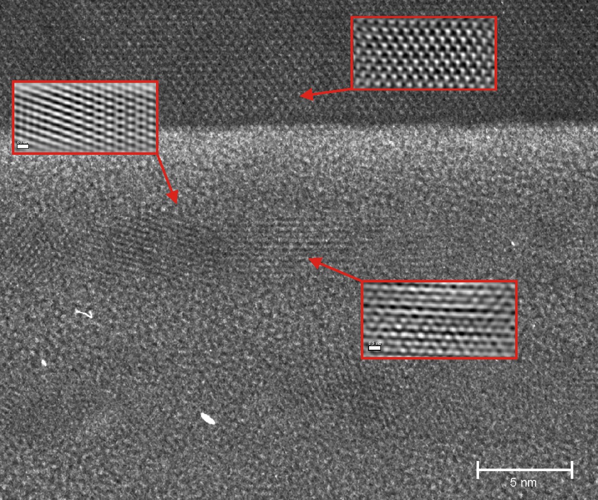
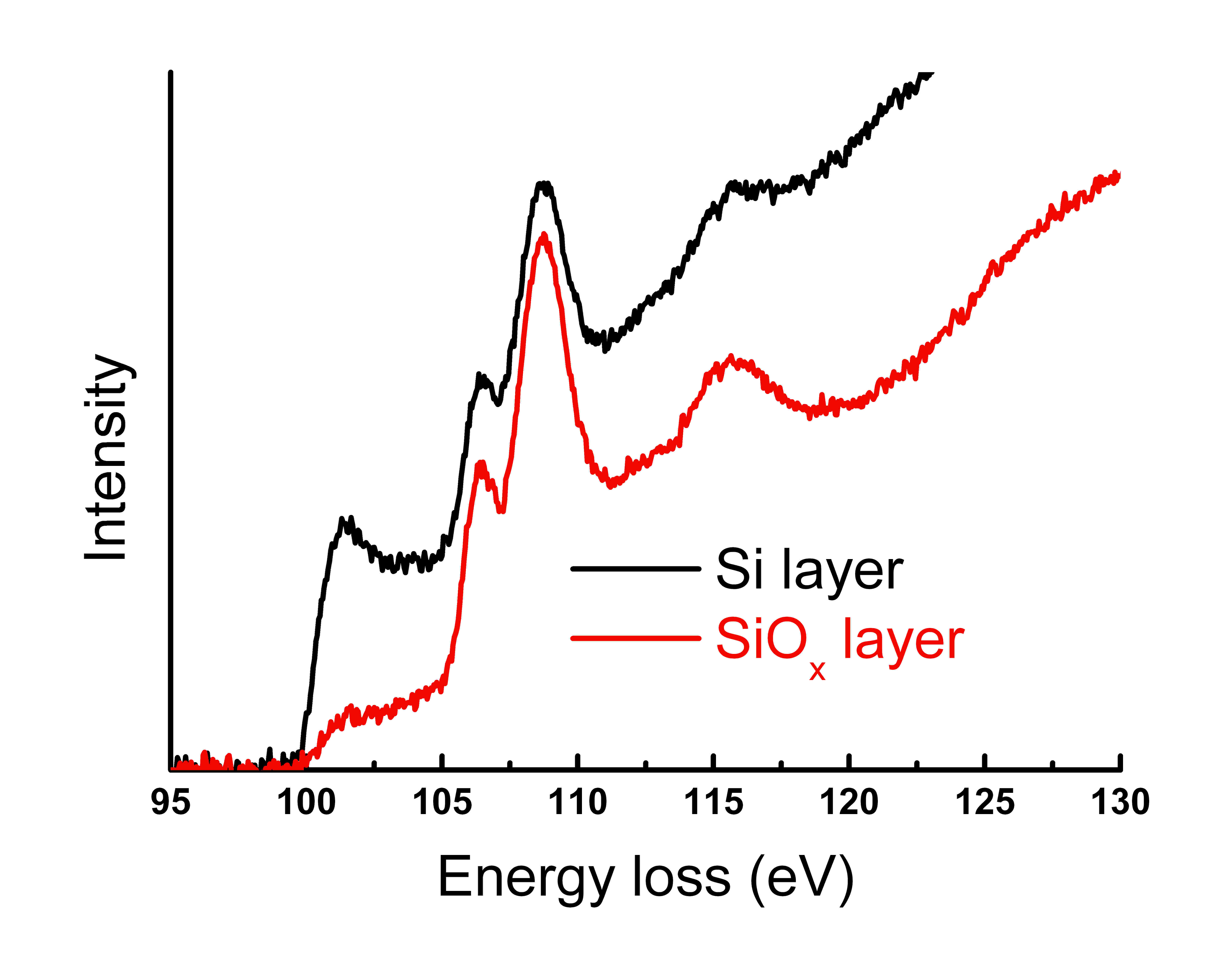
HRTEM and EELS investigations of Si/SiO 2 QW-structures
 |
 |
 |
| EEL-reference spektra of a-Si, bulk Si and SiO2. |
HRTEM-micrograph of QW-structures. The inserts highlight the structre of the crystallites (after digital processing). |
EEL-spektra of regions with and without Si-QW-structures. |
Relevant publications
 |
M. Schade, O. Varlamova, J. Reif, H. Blumtritt, W. Erfurth, H. S. Leipner
High-resolution investigations of ripple structures formed by femtosecond laser irradiation of silicon
Anal. Bioanal. Chem. DOI 10.1007/s00216-009-3342-3 (2009),
|
|
|
Martin Schade, Nadine Geyer, Bodo Fuhrmann, Frank Heyroth, Hartmut S. Leipner
High-resolution analytical electron microscopy of catalytically etched silicon nanowires
Appl. Phys. A 95 (2009), 325-327
|
|
|
M. Schade, F. Heyroth, F. Syrowatka, H. S. Leipner, T. Boeck, M. Hanke
Investigation of the chemical composition profile of SiGe/Si(001) islands by analytical transmission electron microscopy
Appl. Phys. Lett. 90 (2007), 263101
|
Cooperations
contact person: Martin Schade
|
|
|
|