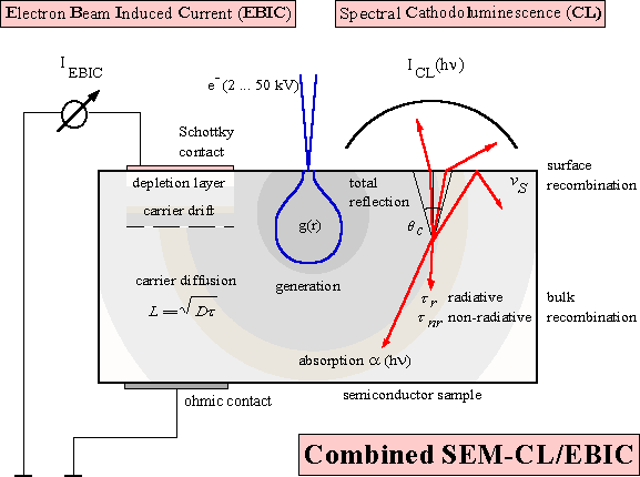
 Figure 1: Scheme of combined SEM-CL/EBIC experiments
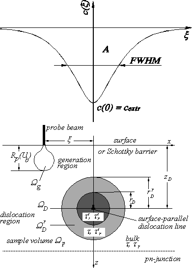 Figure 2:
Schematic configuration of CL/EBIC contrast measurements at a
surface-parallel dislocation
Figure 2:
Schematic configuration of CL/EBIC contrast measurements at a
surface-parallel dislocation
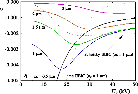
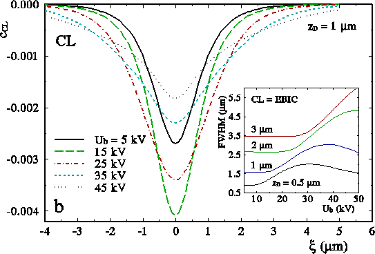 Figure 3: (a) Calculated CL contrast from a surface-parallel
dislocation
for various depths zD (L
= 1 µm,
Figure 3: (a) Calculated CL contrast from a surface-parallel
dislocation
for various depths zD (L
= 1 µm, ![]() = 0.75 µm-1, S
= 0.75 µm-1, S ![]()
![]() ,
, ![]() = 0.01
= 0.01 ![]() ,
, ![]() r
= 0). For zD = 1 µm,
Schottky and p-n EBIC contrasts
are also shown. (b) Corresponding contrast profiles at zD
= 1 µm. The inset shows CL/EBIC profile half-widths as a function
of Ub and zD
r
= 0). For zD = 1 µm,
Schottky and p-n EBIC contrasts
are also shown. (b) Corresponding contrast profiles at zD
= 1 µm. The inset shows CL/EBIC profile half-widths as a function
of Ub and zD
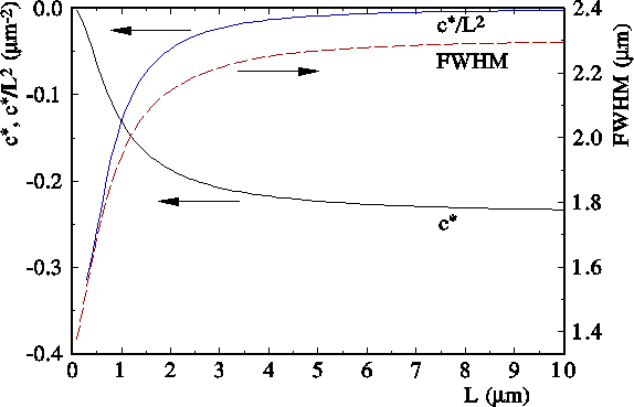 Figure 4: CL
contrast profile function and half-width for varying L
(
Figure 4: CL
contrast profile function and half-width for varying L
(![]() = 0.75 µm-1, S
= 0.75 µm-1, S ![]()
![]() ,
rD = 0.1 µm,
,
rD = 0.1 µm, ![]() r
= 0, zD = 1 µm, Ub
= 20 kV).
Both cCL*
~ c for constant
r
= 0, zD = 1 µm, Ub
= 20 kV).
Both cCL*
~ c for constant ![]() = 0.01 and cCL*/L2
~ c
for constant
= 0.01 and cCL*/L2
~ c
for constant ![]() = 1 are shown
= 1 are shown
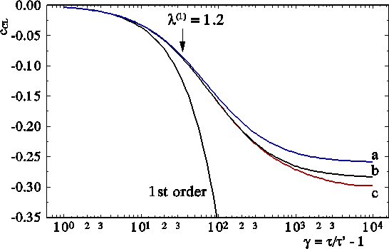 Figure 5 (after [62]):
CL
contrast for varying recombination strength (L = 1
µm,
Figure 5 (after [62]):
CL
contrast for varying recombination strength (L = 1
µm, ![]() = 0.75 µm-1, S
= 0.75 µm-1, S ![]()
![]() ,
rD = 0.1 µm,
,
rD = 0.1 µm, ![]() r
= 0, zD = 1 µm, Ub
= 20 kV) (a)
analytical approximation [62],
(b) series expansion [45],
(c) rotation-symmetric solution [14]
r
= 0, zD = 1 µm, Ub
= 20 kV) (a)
analytical approximation [62],
(b) series expansion [45],
(c) rotation-symmetric solution [14]
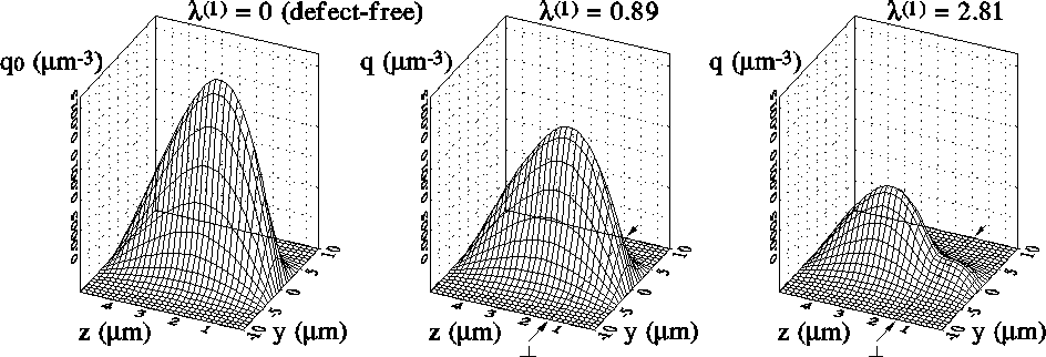 Figure 6:
Numerically calculated excess carrier density q(0,y,z)
for various defect strengths of a surface-parallel line defect
(position
denoted by arrows) in a 5 µm thick layer (L = 3 µm,
S
Figure 6:
Numerically calculated excess carrier density q(0,y,z)
for various defect strengths of a surface-parallel line defect
(position
denoted by arrows) in a 5 µm thick layer (L = 3 µm,
S ![]()
![]() ,
zD = 1.43 µm, Ub
= 20 kV,
,
zD = 1.43 µm, Ub
= 20 kV, ![]() = 2.9 µm)
= 2.9 µm)
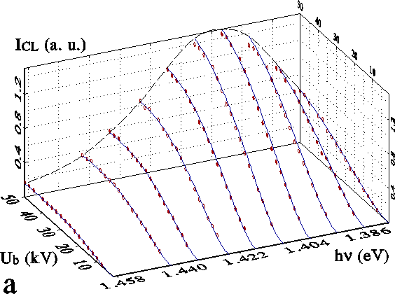
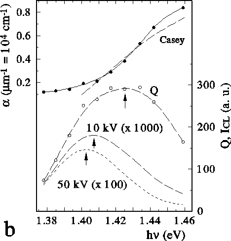 Figure 7 (after [29]):
(a)
Experimental and fitted spectral CL signal (Ub
Ib
= 20 µW) from p-GaAs (L = 4.5 µm, zT
= 0.07 µm, S
Figure 7 (after [29]):
(a)
Experimental and fitted spectral CL signal (Ub
Ib
= 20 µW) from p-GaAs (L = 4.5 µm, zT
= 0.07 µm, S ![]()
![]() ),
(b) Fit results. Top: Absorption coefficient compared with [6],
bottom: Internal spectral distribution and measured CL spectra at Ub
= 10 kV and 50 kV. Arrows denote the spectral maximum positions
),
(b) Fit results. Top: Absorption coefficient compared with [6],
bottom: Internal spectral distribution and measured CL spectra at Ub
= 10 kV and 50 kV. Arrows denote the spectral maximum positions
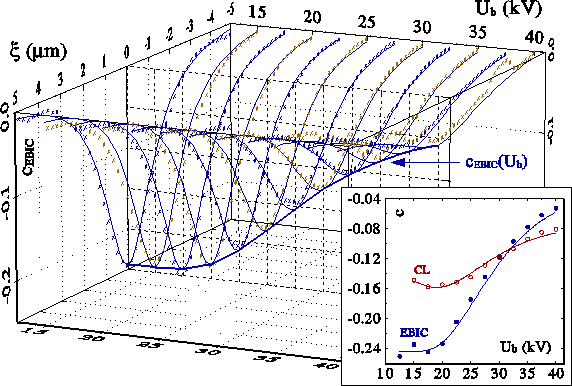 Figure 8 (after [61]):
Experimental
EBIC contrast profiles and best fits for a surface-parallel dislocation
in p-GaAs (
Figure 8 (after [61]):
Experimental
EBIC contrast profiles and best fits for a surface-parallel dislocation
in p-GaAs (![]() = 0.89, zD
= 1.43 µm, L = 3.0 µm). The inset shows the
experimental
and fitted EBIC and CL maximum contrast (
= 0.89, zD
= 1.43 µm, L = 3.0 µm). The inset shows the
experimental
and fitted EBIC and CL maximum contrast (![]() CL
= 0.73)
CL
= 0.73)
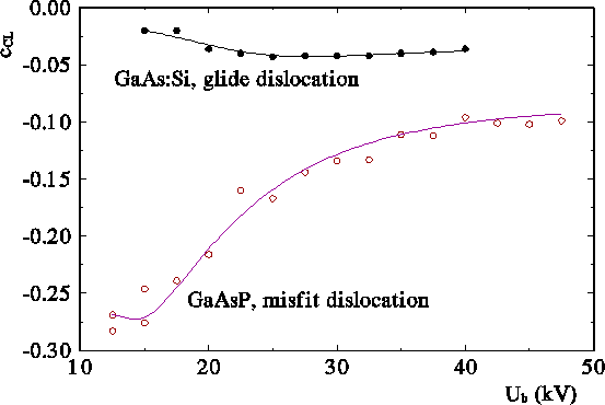 Figure 9:
Experimental and fitted CL contrast from a screw type glide dislocation
in n-GaAs:Si (fit parameters:
Figure 9:
Experimental and fitted CL contrast from a screw type glide dislocation
in n-GaAs:Si (fit parameters: ![]() = 0.95, zD = 1.58 µm, L
= 0.73 µm,
= 0.95, zD = 1.58 µm, L
= 0.73 µm, ![]() = 1.30 µm-1, zT
= 0.03 µm, S
= 1.30 µm-1, zT
= 0.03 µm, S ![]()
![]() )
and a misfit dislocation in n-GaAs0.62P0.38:Te
(
)
and a misfit dislocation in n-GaAs0.62P0.38:Te
(![]() = 1.78, zD = 0.77 µm, L
= 0.90 µm,
= 1.78, zD = 0.77 µm, L
= 0.90 µm, ![]() = 1.08 µm-1, zT
= 0.12 µm, S
= 1.08 µm-1, zT
= 0.12 µm, S ![]()
![]() )
)
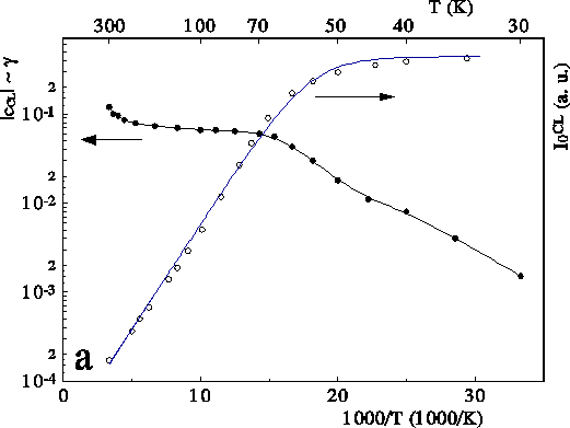
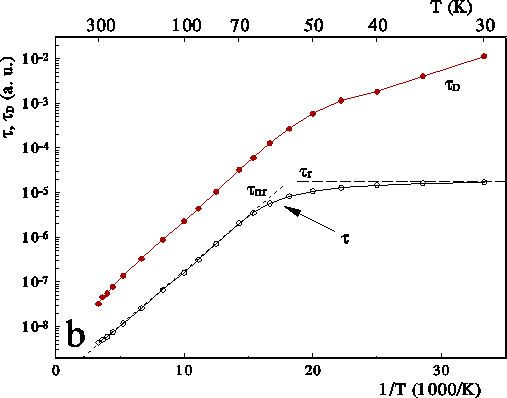 Figure 10: (a) Temperature dependence of the CL contrast of a
surface-parallel
misfit dislocation and the matrix CL intensity in n-GaP (Ub
= 20 kV), (b) Defect and bulk lifetimes as a function of temperature
Figure 10: (a) Temperature dependence of the CL contrast of a
surface-parallel
misfit dislocation and the matrix CL intensity in n-GaP (Ub
= 20 kV), (b) Defect and bulk lifetimes as a function of temperature
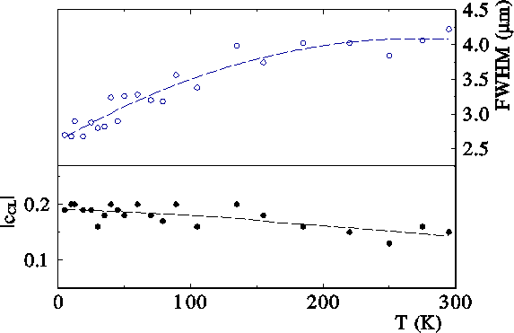 Figure 11:
Temperature dependence of CL contrast and profile half-width
from a threading glide dislocation in n-GaAs (Ub
= 20
kV)
Figure 11:
Temperature dependence of CL contrast and profile half-width
from a threading glide dislocation in n-GaAs (Ub
= 20
kV)
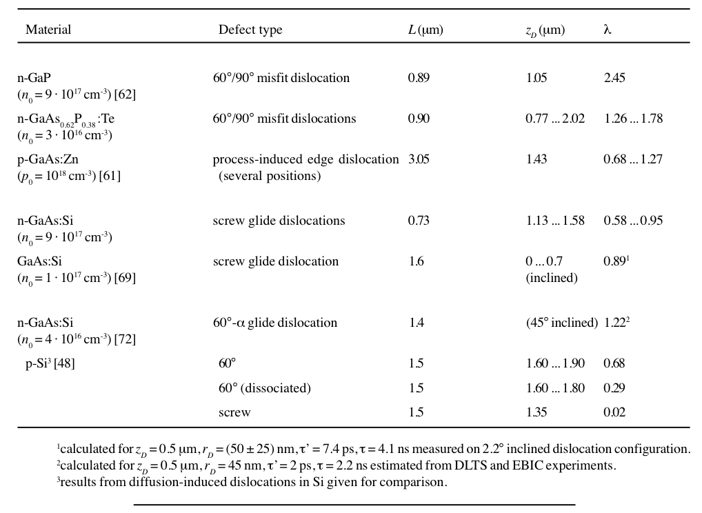
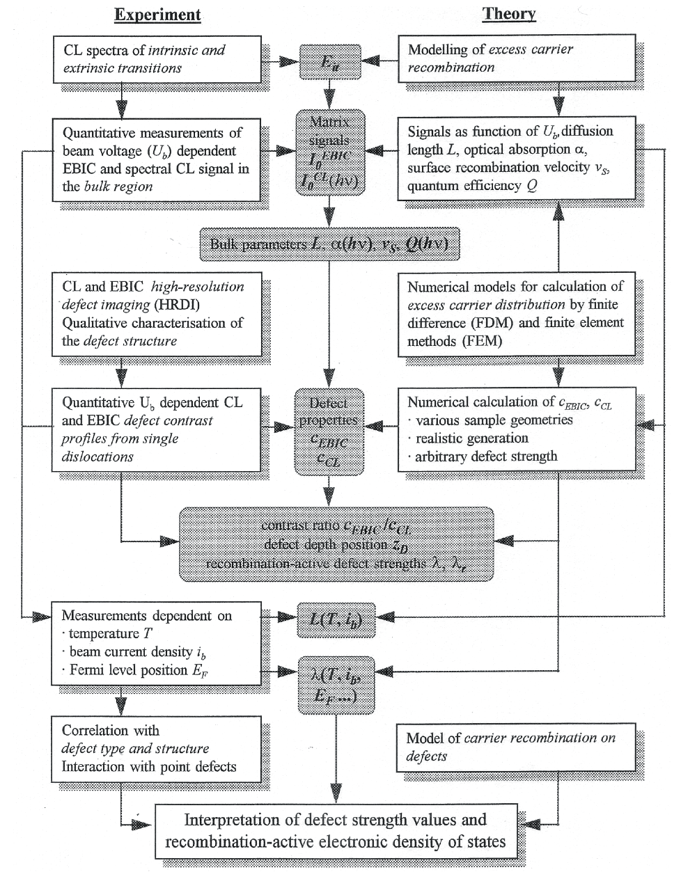 Table 1:
Strategy of SEM/CL-EBIC investigations in semiconductors
Table 1:
Strategy of SEM/CL-EBIC investigations in semiconductors